bg image bg image
bg image bg image what is a ccd linkbasic ccd linkmanufacturing ccds linkWFC3 ccds linkglossary link

Wafer Fabrication :: annealing

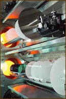
In the annealing process, wafers are heated to a well-defined temperature for a specific amount of time in a conditioned atmosphere (inert, oxidizing, reducing). The temperature, time and type of atmosphere used in an annealing process depends on the purpose of the anneal and the type of surface being treated. Annealing may be used to remove impurities (mostly oxygen) from the surface layers or to cause implanted ions to diffuse further into the silicon.
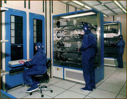
Working at the furnace controls    wafers entering into the furnace  
Next Step :: Ion Implantation
Next Step :: Processing :: Testing

Annealing video link
Annealing Video
Video showing the annealing process from washing to the furnace.

wafers transferring onto platters
Transfering wafers into a carrier to be put into the furnace

Javascript needs to be enabled for the above video link to work. If javascript is not enabled the videos can also be found here.

questions: webmaster@wfc3.gsfc.nasa.gov :: Global Science and Technology :: Credits