|
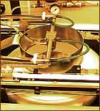
Photolithography is the process by which
structures of different size and shape are created on
the wafers. The wafers are first coated with photoresist,
a polymer that is sensitive to ultraviolet light. The
wafers are then exposed to UV light through a mask, which
acts like a stencil; only letting light hit the wafers
in certain places to form a pattern. Photoresist polymers
can be created so that UV light either weakens or strengthens
the polymer, so that when the photoresist is developed,
the weaker material is washed away, leaving behind the
desired pattern.
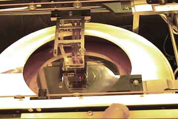
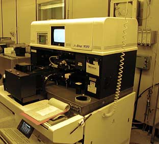
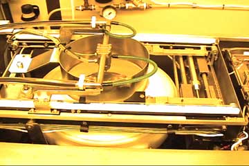
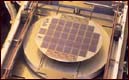
| Applying Photoresist |
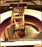
Applying the Mask |
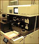
Applying Developer |
|
|
 |
Previous Step :: deposition
Next Step :: etching
|