|
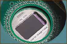
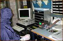
After the wafers come from fabrication,
the first series of tests they go through are called DC tests.
These are electrical tests to check the electrical connections
of each of the devices on the wafers. If the wafers pass the
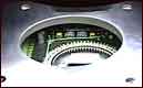
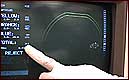
initial DC tests they go on to the image probe test. This
is a functional test to roughly assess the imaging capability
of each device. The devices are graded according to their
image quality. Wafers containing poor quality devices are
not processed any further. The criteria for judging science
grade devices are of course more stringent than the criteria
for making devices for other purposes.
| Image Probe test |
Electrical Probe test |
|
 |
Previous Step :: Processing :: annealing
Next Step :: backthinning
|