|
Backthinning is just what it sounds like,
literally thinning the backs of the devices. Backthinning
is done because most customers with scientific requirements
require the absolute maximum performance and sensitivity
in the devices.
In order to use every last photon of light that is available,
the best thing to do is to turn the ccd over and shine
the light through the back. Unfortunately because of the
thickness of silicon a lot of performance is lost before
the light gets to the part that works. In order to minimize
that effect we have to remove a major part of the silicon
from the back side of the surface until it is about 15
microns. This is about the thickness of a human hair and
very high sensitivity and performance are achieved.
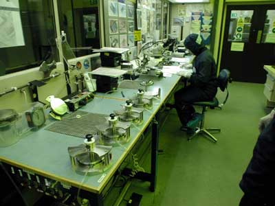
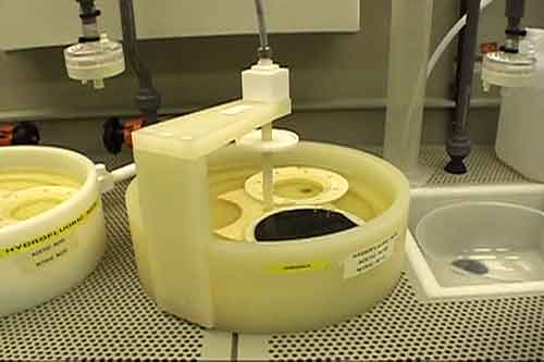
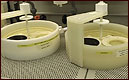
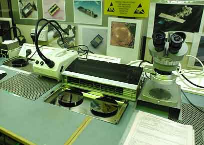
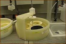
The wafers are first attached to support wafers (pictured
below) and then thinned. A common process of thinning
the wafers is for them to be immersed in an acid bath.
The acid eventually thins the wafers down to their desired
thickness.
 Previous Step :: Testing
Next Step :: Coating
|