bg image bg image
bg image bg image what is a ccd linkbasic ccd linkmanufacturing ccds linkWFC3 ccds linkglossary link

Wafer Fabrication :: assembly

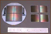
After the wafers are thinned they need to be assembled. Depending on the size of the CCD several devices may be on a single CCD wafer. The first step in the assembly process is for them to be cut into their 
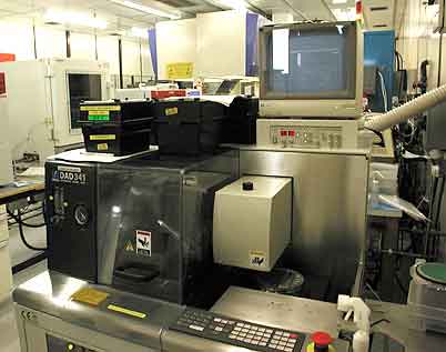
individual devices. The cutting is done with a computer programmed dicing saw.

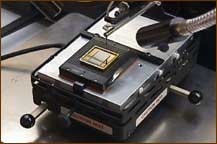
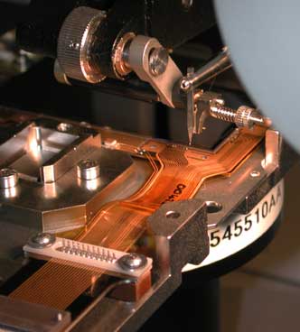
After the wafers are diced they must be bonded down onto the chip pad. The diced CCD is wired bonded onto the chip pad. Then this pad is bonded down onto a board pad. The board pad is a piece of board which makes up the CCD package. Once the bonding process is done it is then inspected to make sure everything was done correctly.
Wafers after being Diced Wire Bonding
diced wafers wire bonding
Dicing Saw Close up of WFC3 Wire Bonding
dicing saw wire bonding close up
Top images courtesy of University of Arizona Imaging Technology Laboratory
Previous Step :: coating
Next Step :: testing


assembly video link
Assembly Video
Video showing you the dicing saw, chip pad bonding, and inspection.


diagram of a ccd
diagram of a CCD
Breakdown of the parts in a CCD.

Javascript needs to be enabled for the above video link to work. If javascript is not enabled the videos can also be found here.

questions: webmaster@wfc3.gsfc.nasa.gov :: Global Science and Technology :: Credits