|
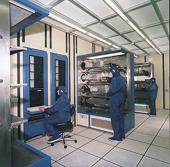
The CCD manufacturing process can be divided into 2 major stages,
wafer fabrication and post-processing.
Wafer Fabrication
Wafer fabrication is the process by which different electrical
components and structures are placed on the silicon wafers
to produce CCDs. The entire process is typically done
in batches of about 20 wafers at a time. Each wafer may
contain from two to several dozen CCDs, depending on the
size and format of the devices being fabricated. Five
basic processes are used in the wafer fabrication stage
and may be repeated several time in order to make the
desired devices.
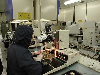
Post Processing
After completion of wafer fabrication, the wafers are ready for
post processing, which consists of 5 major activities
|